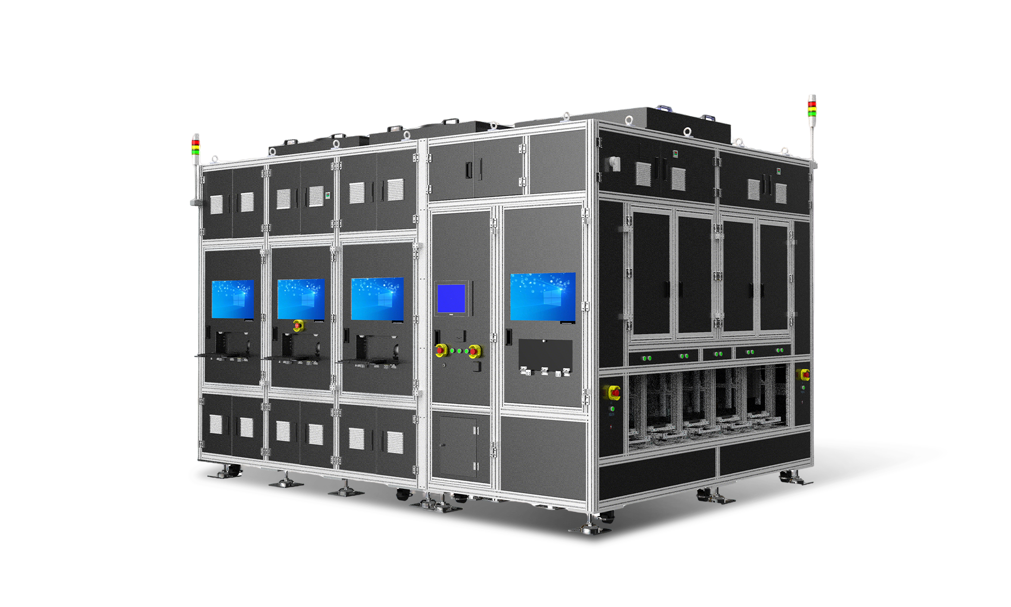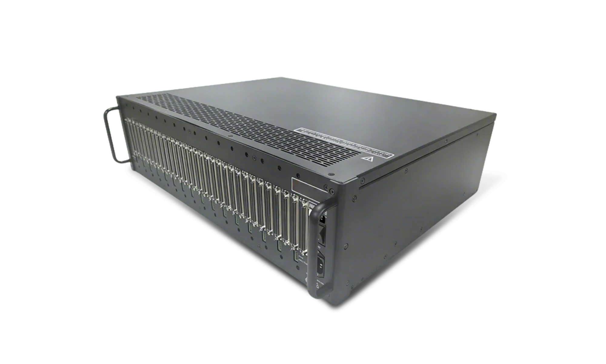




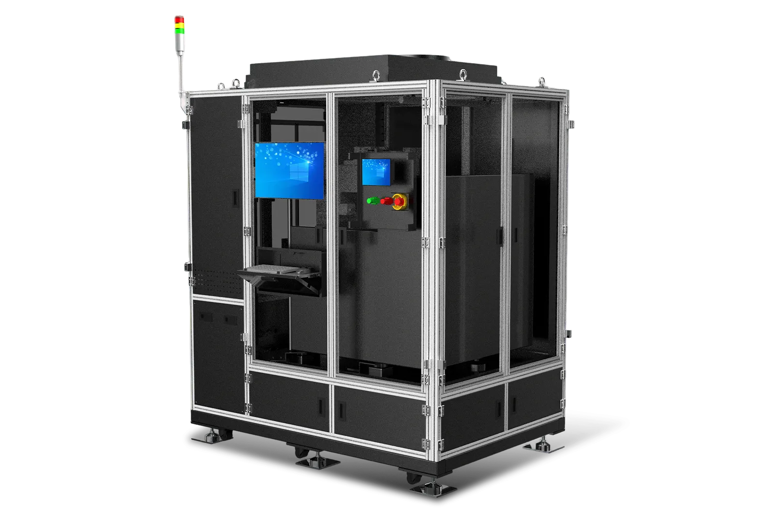
Wafer Automated Optical Inspection
For the optical, electrical, and other properties of silicon-based Micro LED/OLEDs after power-on, this is a fully automated system for image capture, analysis, and testing. It is used for display function and defect detection during the power-on process of the cell segment before Micro LED dicing.
Scroll to Explore
Product Advantages
-
01High-resolution optical system enables detection of pixels with a pitch as small as 2.5 μm
-
02With a fully automatic optimized design, it enables high-speed detection. Wafer AOI test: TT <15 sec/DIE
-
03High-accuracy algorithm design delivers grading accuracy ≥99%
Product
Features
1. Micro LED/OLED Wafer screen detection after power-on
2. Test items include brightness, wavelength, dead spot, dark spot, bright spot, etc.
3. Can be connected to automatic feeding systems and MES